



Semiconductor Ecosystem / Odisha Signs Semiconductor Pact with Intel, 3DGS to Boost Substrate Manufacturing
Key Points
- Odisha govt signs MoU with Intel & 3DGS.
- Rs2,000 crore project to manufacture 70,000 panels annually.
- Odisha hosts India’s first 3D chip packaging unit.
- Semicon India approves 12 fab projects, 24 design projects.
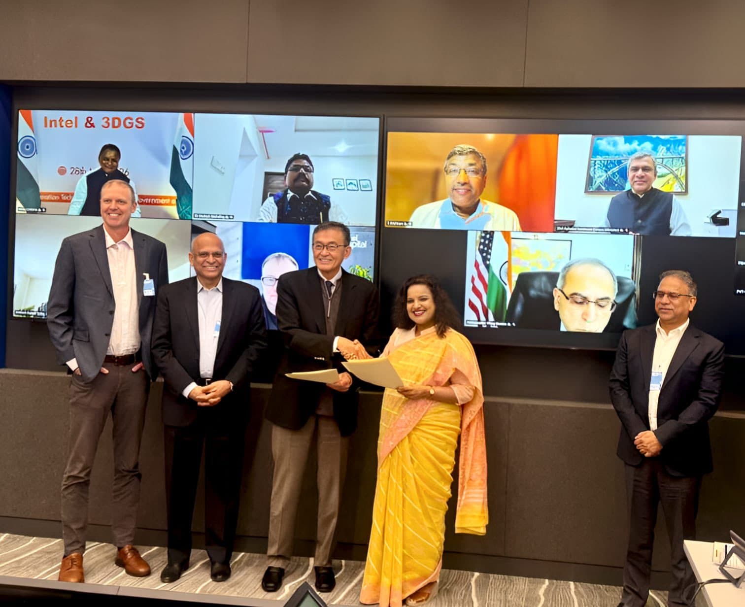
New Delhi/Bhubaneswar, May 29: The Odisha government signed a memorandum of understanding (MoU) with Intel and 3D Glass Solutions (3DGS) to bring advanced substrate manufacturing technology to India, officials said on Friday.
Congratulating the state government and its partners, Union
Minister for Electronics and Information Technology Ashwini Vaishnaw said the
pact would further strengthen India’s semiconductor ecosystem.
“Congratulations to the Govt. of Odisha, Intel and 3DGS on
signing an MoU to bring substrate manufacturing technology to India. This will
further advance the semiconductor ecosystem in India,” he posted on X.
Congratulations to the Govt. of Odisha, Intel and 3DGS on signing an MoU to bring substrate manufacturing technology to India.
This will further advance semiconductor ecosystem in India. pic.twitter.com/elxs6r8muN

📱 Get Argus News App
✨
The agreement builds on Odisha’s broader semiconductor push
announced earlier this year. In April, the foundation stone was laid for
India’s first advanced 3D chip packaging unit at Info Valley in Bhubaneswar
under the Heterogeneous Integration Packaging Solutions project promoted by
3DGS.
The project involves an investment of nearly Rs2,000 crore
and is expected to manufacture around 70,000 glass panels annually, along with
50 million assembled units and nearly 13,000 advanced 3D heterogeneous
integration (3DHI) modules, according to government estimates.
Union Minister Vaishnaw earlier noted that under Prime
Minister Narendra Modi’s leadership, India’s semiconductor sector is witnessing
rapid growth, with Odisha emerging as a key contributor.
Chief Minister Mohan Charan Majhi also highlighted that
Odisha is the only state where both India’s first compound semiconductor
fabrication unit and first 3D glass substrate packaging facility are being
established.
Also Read: Odisha Emerging As Semiconductor Hub, Says CM Majhi At 3D Glass Unit Groundbreaking
The development comes as the Centre continues to strengthen
the domestic semiconductor ecosystem through policy support and incentives
under the Semicon India Programme. Earlier this week, the government announced
that 12 fab or packaging projects and 24 semiconductor design projects have
already been approved. Additionally, an online Investor Support portal has been
launched to boost investor confidence and address industry concerns.
With Odisha’s latest pact, India takes another step toward
building a robust semiconductor supply chain, positioning itself as a global
hub for advanced electronics manufacturing.
Related Topics
Explore more stories