



From Steel to Silicon Value Chain: Why Modi's ₹1.27-Lakh-Crore Semicon 2.0 Could Give Odisha Its Biggest High-Tech Opportunity Yet | Special Report
Key Points
Bhubaneswar: When the Union Cabinet on Wednesday approved Semicon 2.0 with a massive Rs1.27 lakh crore outlay, much of the national conversation revolved around India's ambition to emerge as a global semiconductor manufacturing hub.
For Odisha, however, the policy marks something far more significant.
Unlike Gujarat, Karnataka or Tamil Nadu, Odisha is not entering the semiconductor race with decades of electronics manufacturing, chip fabrication or consumer electronics ecosystems. Yet, paradoxically, that may now work to its advantage.
Semicon 2.0 fundamentally changes India's semiconductor strategy.

📱 Get Argus News App
✨While the first phase largely revolved around attracting mega fabrication plants, Semicon 2.0 recognises that the semiconductor industry is an interconnected ecosystem – from chip design and research to advanced packaging, speciality materials, equipment and skilled manpower.
That broader approach opens multiple entry points for emerging states like Odisha.
The real question, therefore, is not whether Odisha can compete with Gujarat's silicon fabs. It is whether the state can carve out a specialised role within India's semiconductor value chain.
The answer increasingly appears to be yes.
Why Semicon 2.0 Changes Odisha's Equation
India has already approved 12 semiconductor manufacturing projects worth over Rs1.64 lakh crore under Semicon 1.0, including one silicon fab, one silicon carbide fab, an integrated Gallium Nitride Micro LED Display Fab and nine packaging facilities.
Three companies – Micron, Kaynes and CG Semi – have already entered commercial production.
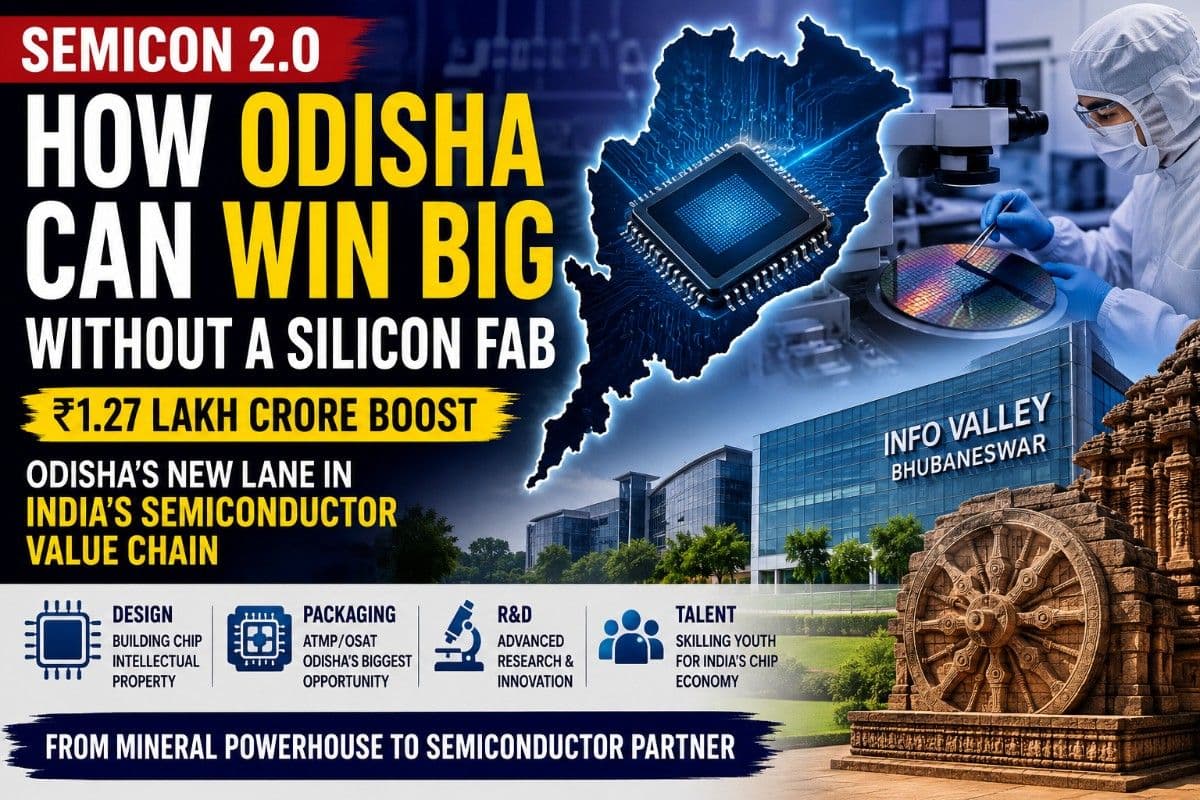
Semicon 2.0 builds on that momentum by expanding support across six pillars – design, machines and materials, fabrication, ATMP/OSAT packaging, research and talent development.
For Odisha, however, not all six pillars carry equal significance.
Some offer transformational opportunities.
Others remain long-term possibilities.
Pillar One: Odisha Can Build a Chip Design Ecosystem Without Building a Fab
One of the most significant shifts under Semicon 2.0 is the emphasis on semiconductor intellectual property (IP).
The Centre plans to deepen India's chip-design ecosystem after already supporting over 100 startups working on indigenous semiconductor designs.
This directly complements Odisha's emerging technology ecosystem centred around IIT Bhubaneswar, IIIT Bhubaneswar, OUTR, VSSUT and the semiconductor ecosystem taking shape in Info Valley.
Traditionally, Odisha has produced engineering graduates who migrate to Bengaluru, Hyderabad or Pune for semiconductor jobs.
Semicon 2.0 creates the possibility of reversing that trend.
As semiconductor companies establish design centres closer to manufacturing and packaging facilities, Odisha can gradually evolve into a producer of chip architects, verification engineers, embedded system developers and AI-chip designers rather than remaining merely an exporter of engineering talent.
For a knowledge economy, intellectual property generates significantly greater long-term value than manufacturing alone.
Pillar Four Could Become Odisha's Biggest Opportunity
Among all six pillars, the strongest immediate opportunity for Odisha lies in ATMP (Assembly, Testing, Marking and Packaging) and OSAT (Outsourced Semiconductor Assembly and Testing).
Globally, semiconductor packaging has undergone a technological revolution.
Advanced chips increasingly depend on sophisticated packaging technologies such as 3D integration, heterogeneous packaging and compound semiconductors rather than conventional assembly methods.
Importantly, Odisha's semiconductor roadmap is already moving in this direction. The State has recently signed mous with intel, 3D Glass Solutions to to establish an advanced semiconductor glass core substrate manufacturing facility in the Bhubaneswar-Khurda region.
Unlike traditional silicon wafer fabrication plants that require investments running into billions of dollars along with ultra-mature electronics ecosystems, advanced packaging facilities require comparatively lower capital, shorter implementation periods and a different industrial ecosystem.
Semicon 2.0 explicitly incentivises this segment.
That substantially improves Odisha's competitiveness.
Instead of attempting to replicate Gujarat's silicon fabrication model, Odisha can emerge as a specialised destination for advanced semiconductor packaging – one of the fastest-growing segments of the global semiconductor industry.
That niche positioning may ultimately prove more sustainable than competing head-on for mega fabs.
Pillar Five Strengthens Odisha's Research Ambition
Semiconductor manufacturing evolves rapidly.
Technologies that are cutting-edge today become obsolete within a few years.
Recognising this, Semicon 2.0 significantly expands support for semiconductor research and advanced technology development.
For Odisha, this strengthens efforts to build a research-led semiconductor ecosystem through institutions such as IIT Bhubaneswar and future industry-academia collaborations.
Instead of limiting itself to manufacturing support services, Odisha now has an opportunity to participate in prototype development, semiconductor testing, compound semiconductor research and emerging chip technologies.
That transition – from manufacturing support to technology development – could become one of the state's biggest long-term gains.
Pillar Six Can Retain Odisha's Engineering Talent
Perhaps the most visible social impact will come from talent development.
The Government has already trained around 68,000 students across 315 universities using industry-standard Electronic Design Automation (EDA) tools.
Semicon 2.0 now expands that effort further by focusing on clean-room operations, fab construction, semiconductor equipment maintenance and advanced packaging technologies.
This aligns well with Odisha's expanding engineering education ecosystem.
Instead of producing graduates who leave the state immediately after graduation, Odisha can begin creating a specialised semiconductor workforce capable of supporting industries emerging within the state.
That would gradually strengthen the state's high-value employment ecosystem.
Pillar Two Offers Opportunity – But Not Through Odisha's Minerals
One area requires careful distinction.
Semicon 2.0 incentivises companies manufacturing semiconductor machinery, speciality chemicals, industrial gases and advanced materials.
However, this should not be confused with Odisha's traditional mineral strengths.
The semiconductor industry depends on ultra-high-purity silicon, speciality gases, electronic chemicals and precision materials—not on iron ore, bauxite or coal that have historically powered Odisha's industrial economy.
Odisha's advantage, therefore, lies elsewhere.
The state possesses extensive industrial land banks, reliable industrial power, water infrastructure, chemical manufacturing experience and established industrial regulatory systems.
These capabilities make Odisha a potential destination for companies manufacturing semiconductor-grade chemicals, speciality gases and precision industrial materials that will serve fabs located across India.
In other words, Odisha's opportunity is to host new semiconductor-support industries, not because it possesses semiconductor minerals, but because it already possesses the industrial ecosystem required to establish them.
That distinction is crucial.
Why Odisha Need Not Chase Silicon Fabs
Much public attention inevitably focuses on semiconductor fabrication plants.
They represent the most visible symbols of technological advancement.
Yet they are also among the world's most capital-intensive manufacturing facilities, requiring mature electronics supply chains, highly specialised vendor ecosystems and enormous financial commitments.
Today, Gujarat enjoys a significant first-mover advantage in this segment.
Tamil Nadu possesses deep electronics manufacturing capabilities.
Karnataka continues to dominate semiconductor design.
Odisha does not need to replicate their strengths.
Semicon 2.0's ecosystem approach allows different states to specialise in different segments of the value chain.
That is precisely where Odisha's strategy appears most realistic.
Odisha's Semiconductor Future Lies in Specialisation
If Semicon 1.0 rewarded states capable of attracting mega fabs, Semicon 2.0 rewards states capable of integrating into the broader semiconductor ecosystem.
For Odisha, that means building comparative advantages in four areas:
- Advanced semiconductor packaging (recently signed mous with intel, 3D Glass Solutions) and ATMP/OSAT facilities.
- Compound semiconductor technologies and emerging chip applications.
- Semiconductor research, design and innovation.
- A specialised talent pipeline for India's growing chip industry.
This strategy demands far lower capital than conventional silicon fabs while allowing Odisha to participate in one of the world's fastest-growing technology sectors.
For decades, Odisha's industrial identity has been shaped by steel, aluminium and mining.
Semicon 2.0 does not rewrite that history overnight.
But it offers the state an opportunity to add an entirely new chapter – one where Odisha is recognised not merely as India's mineral powerhouse, but as a specialised contributor to the country's semiconductor economy.
That may
ultimately become the policy's most enduring impact on the state.
Also Read: Intel 3DGS Mega Push / By 2031, Odisha Could Power India’s 5G and 6G Future – Big Opportunity for Odia Tech Talent| Exclusive Analysis
Related Topics
Explore more stories